
HBM Memory

Post-HBM4 Roadmap: A Forward Look at HBM4E and HBM5 Specs
As HBM4 moves from pilot to early volume, industry attention is already shifting toward the next logical stages: evolutionary refinements sometimes labeled HBM4E and a more disruptive generational step often discussed under the HBM5 moniker. This post surveys likely technical directions, realistic performance and integration targets, key enabling technologies, supply-chain and manufacturing implications, and design trade-offs system architects should expect over the next 3–6 years.

The Structurally Upward Shift in Memory ASP Driven by HBM
High Bandwidth Memory (HBM) has become a defining technology in modern computing architectures. As HBM adoption grows across GPUs, AI accelerators, and high-performance CPUs, it is doing more than just increasing raw throughput. HBM is driving a structural upward shift in the memory Application Service Profile (ASP)—the way systems expose, package, and price memory as part of broader computing platforms.

Analyzing the Possibility of New Entrants Challenging the HBM Oligopoly
High Bandwidth Memory (HBM) has become central to high-performance computing, AI accelerators, and advanced graphics. Its market is currently dominated by a small number of players with deep expertise in DRAM design, advanced packaging, and system-level integration. This concentration has led many to describe HBM as an oligopoly.

A Full Mapping of HBM-Themed Targets in the A-Share Market
As High-Bandwidth Memory (HBM) becomes a core enabler for AI, high-performance computing and advanced graphics, China’s domestic capital markets have seen a rapid expansion of “HBM concept” stocks and supply-chain plays. While the most advanced HBM die and module production remains concentrated in Korea and the United States, a growing number of A-share listed companies participate in the broader HBM ecosystem—through equipment, materials, packaging, substrates, thermal solutions, and peripheral components.

The Layer Stack and Thermal Bottleneck Breakthroughs in the HBM3E-to-HBM4 Upgrade
Upgrading from HBM3E to HBM4 represents one of the most technically challenging—and most consequential—evolutions in modern memory engineering. HBM4 promises higher signaling rates, greater per-die capacity, and improved energy efficiency per bit, but achieving those gains requires rethinking the layer stack, interconnect strategies, and thermal management at the package level.

Tracking the Spot vs. Contract Price Spread Dynamics in HBM Market
High-Bandwidth Memory (HBM) has transitioned from a boutique, high-margin specialty to a strategic commodity within high-performance computing and AI infrastructure. That transition created two distinct pricing channels: spot-market transactions (ad-hoc purchases, inventory sales, and opportunistic trades) and contract-based procurement (multi-year supply agreements, prepayments, and capacity reservations).

2027 HBM Market Size Forecasts: The Upper/Lower Bound Divergence Among Major Institutions
High Bandwidth Memory (HBM) has transitioned from a niche technology to a central pillar of the AI and high‑performance computing ecosystem, and by 2027 it is expected to sit at the heart of GPU, accelerator, and advanced CPU platforms worldwide. Against that backdrop, financial institutions and industry research houses have been racing to forecast the market size for HBM, yet their estimates vary widely. Some project an aggressive, multi‑fold expansion with tight supply and premium pricing, while others caution that bottlenecks and substitution effects could cap growth.

2026 HBM Supply-Demand Gap Forecast: How Much Shortfall Remains?
High‑Bandwidth Memory (HBM) is now a critical component across AI training clusters, inference accelerators, and high‑performance computing systems. As demand surged between 2022 and 2026, suppliers scrambled to expand wafer capacity, interposer production, advanced packaging, and specialized test and burn‑in capacity. Yet multiple bottlenecks—packaging throughput, materials, tooling lead times, and yield learning—left the market short of fully meeting demand.

The Irreplaceability of Japanese Material Suppliers in the HBM Supply Chain
High-Bandwidth Memory (HBM) has quickly become a strategic pillar of modern AI, HPC, and accelerator architectures. Behind the headlines about wafers, interposers, and packaging capacity lies a quieter but crucial reality: a small cluster of highly specialized Japanese material suppliers provides many of the chemicals, precision films, specialty substrates, and consumables that enable reliable, high-yield HBM production.
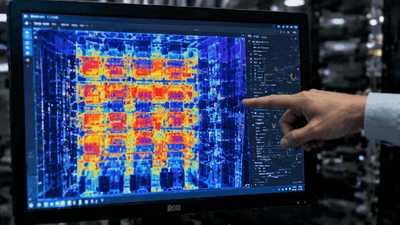
HBM Power Consumption and Thermal Issues Become Core System-Level Design Bottlenecks
High-Bandwidth Memory (HBM) has become essential for modern AI accelerators and high-performance compute nodes because it delivers massive on-package bandwidth and high energy efficiency per bit transferred. Yet as HBM stack counts, per-die speeds, and module counts per accelerator increase, power consumption and thermal management move rapidly from component-level concerns into system-level bottlenecks.
Popular

Narrowing Spread Between NAND Spot and Contract Prices in 2026 – A Signal
By 2026, one of the most watched metrics in the NAND flash market has started to shift in a subtle but meaningful way: the spread between spot prices and long‑term contract prices is narrowing. For casual observers, this may look like just another incremental change in a notoriously volatile industry. For memory makers, module houses, device OEMs, and data center buyers, however, a tightening gap between spot and contract prices is a signal—a reflection of evolving supply–demand balance, risk perceptions, and strategic behavior on both sides of the market.

Price Divergence Trading Strategies Between NAND Flash and DRAM ETFs
NAND flash and DRAM sit at the core of AI storage and computing power. Both are memory, but they are not the same business. DRAM is main memory—fast, volatile, and central to high‑bandwidth workloads like AI training and inference. NAND is non‑volatile storage—slower than DRAM, but crucial to persistent data and large‑scale object storage. The cycles that drive their pricing and margins overlap, yet they often diverge. That divergence is where trading strategies between NAND and DRAM ETFs become interesting.

China’s HBM Localization Progress: The Catch-Up Pace of CXMT and XMC
China’s drive to localize advanced memory technologies has accelerated over the past several years. High-Bandwidth Memory (HBM) sits near the center of that strategy because it is integral to AI accelerators, high-performance computing (HPC) and other strategic compute platforms. Two domestic players—ChangXin Memory Technologies (CXMT) and XMC (Xianghui Memory, commonly referred to as XMC)—have become focal points in assessing how quickly China can close the gap with international incumbents on HBM die, stacking, and packaging.